
- Contact Us
- Hot line:86-0755-83952193
Mob:+8613632905958
Email:jw@pcjoinwin.com
Skype:joinwin1
Add:Room 906, 9/F Bantian Group commerical center, No. 20. LiShipai. Bantian Street, Longgang district, Shenzhen. China.
- Our Products
- Your position:Home > Our Products > PC ddr3 ram > desktop ram ddr3 2gb with ETT .....
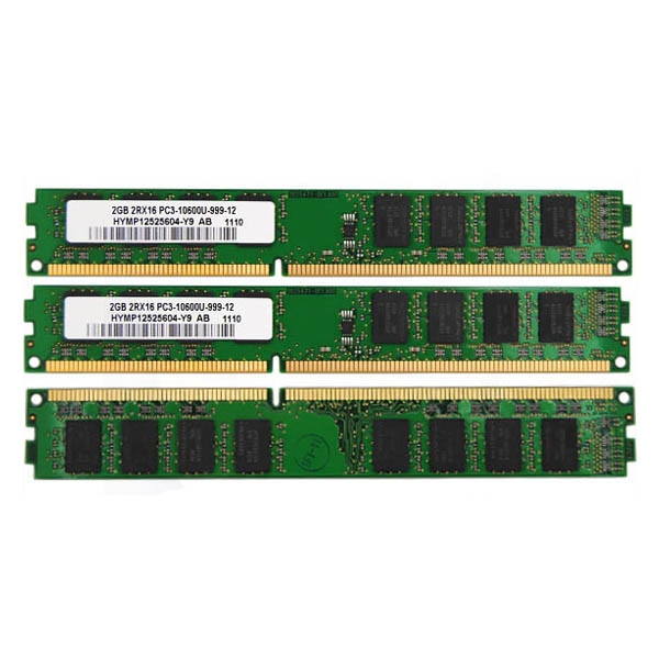

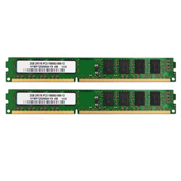
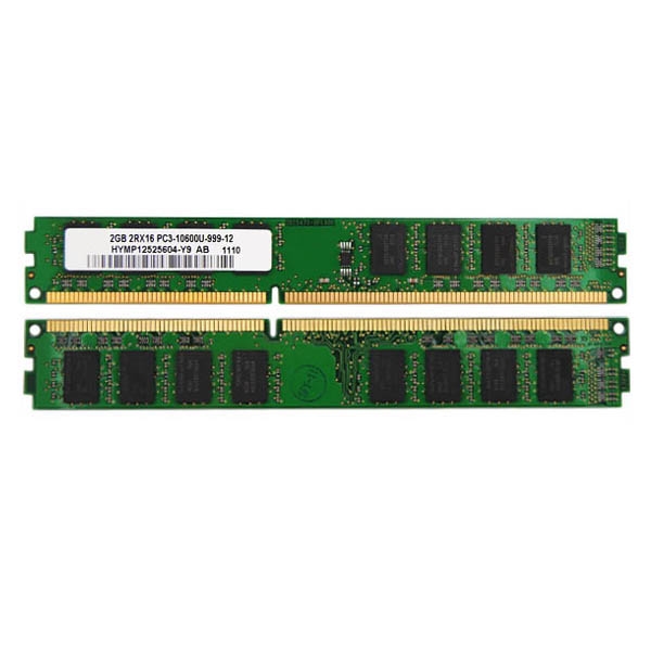


desktop ram ddr3 2gb with ETT original chips tested full compatible
- ETT original chips tested full compatible desktop ram ddr3 2gb
- Original chipsets ETT
- 2gb ddr3 ram memory,tested
- FCC CE RoHS
Memory Type: DDR3
Memory Speed: 1066/1333/1600MHz DDR3
Memory Size: 1GB/2B/4GB/8GB
Memory Channels: Dual
Memory Socket: LONG DIMM
Memory CAS Latency: 4-4-4-12
Memory Timing:4-4-4-12
Pins:240pin
Voltage:1.5V
Function: Non ECC Memory
Chip: Original chips ( brand new )
Warranty:Life time
Detail Description:
1) DDR 400/333 & DDRII 533/667/800 & DDR3/1066/1333/1600 MHz.
2) 168/184/240-pin socket type dual in line memory module (DIMM) .
3) 2.6V power supply
4) Data rate: 400/333/533/667/800M1066/1333MHZ/1600mhz (max).
5) 2.5 V (SSTL-2 compatible) I/O for DDR I products, 1.8Vpower supply for DDR II products
6) Double-data-rate architecture, two data transfers per clock cycle.
7) Bi-directional, differential data strobe (DQS) is transmitted/received with data, to be
used in capturing data at the receiver
8) Data inputs and outputs are synchronzed with DQS.
9) DQS is edge aligned with data for read, center aligned with data for write.
10) Differential clock inputs (CK and CK).
11) DLL aligns DQ and DQS transitions with CK transitions
12) Commands entered on each positive CK edge: Data and data mask referenced to both edges of DQS.
13) Four internal banks for concurrent operation (component).
14) Data mask(DM) for write data.
15) Auto precharge option for each burst access
16) Programmable burst length: 2, 4, 8
17) Programmable/CAS latency (CL): 3
18) Programmable output driver strength: Normal/weak
19) Refresh cycles: (8192 refresh cycles/64ms) .
20) 7.8US maximum average periodic refresh interval.
21) Posted CAS by programmable additive latency for better command and data bus efficiency
22) Off-chip-driver impedance adjustment and on-die-termination for better signal quality .
23) DQS can be disabled for single-ended data strobe operation
24) 2 variations of refresh
